Of all countries, USA is by far the largest consumer of energy. In 2001 about 36 Quads of electricity was produced in the US at a cost of nearly $525 billion. 20% of that energy was used for lighting alone, leading to cost of nearly $50 billion. The existing sources of light are inefficient, with the typical incandescent light bulb consuming 45% of all lighting energy, and only producing 14% of produced light. Aobut 90% of energy goes to the production of heat, leading to excessive costs and pollution from power generation. One of the new lighting technlogies which emerged within the past two decades and has the potential of becoming more energy-efficient than the existing light sources is the solid-state lighting technology of Organic Light Emitting Diodes (OLEDs).
A "small molecule" solar cell consists of a series of very thin vapor deposited organic layers sandwiched between two electrodes, a transparent anode (Indium Tin Oxide) and a metallic cathode on top. Two types of electrodes are used -- an extremely layer of indium tin oxide (becuase it has to be optically transparent), is used as an anode. Low work-function metals such as magnesium, lithium, and their alloys with silver and aluminum are now used as cathodes. While there is no restriction on the size and shape of OLED devices, and every conceivable shape and form can be envisioned, only human synthetic capability is the limiting factor. The deivces can be in the form of fibers, woven to fabrics, bent or rolled as films on curved surface. The near two dimensional nature of OLEDs will represent a new paradigm shift and it may take some time before it is publically acceptable.
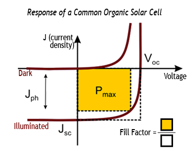
Under dark conditions the cell shows a diode behavior with a characteristic rectification ratio. When light is shined to the device the current is raised at reverse bias, this is called photocurrent. The most important parameters on this cell are the Voc (voltage at open circuit); Jsc (current density at short circuit); the Fill Factor (FF) that is a measure of the quality of the cell (the closer to 1 the better) and the Pmax that is the maximum power that can be obtained from this cell. CuPc (copper phtalocianine) is normally used as the donor layer. C60 is a very good acceptor layer. BCP (Bathocuproine) is commonly used as the "buffer" layer.
Process Overview: The basic mechanism of photocurrent generation in organic photovoltaic cells (OPVs) can be illustrated with two organic materials, one a net electron donor (D) and the other an acceptor (A). The animation below outlines the process involved with the inner workings on a typical polymer cell.
Light Absorption: The first step of the process is light absorption, leading to exciton formation.The exciton can be formed in either the donor or acceptor layer, and is illustrated for the donor layer here. In order to cover a large fraction of the solar spectrum, the donor and acceptor materials chosen for OPVs have broad absorbance lines and high extinction coefficients, giving a high optical density for thin films.
Exciton Diffusion: Once formed, the exciton then migrates to the D/A interface, or alternatively decays to the ground state via radiative or nonradiative processes. The optimal thickness is determined by the exciton diffusion length, since excitons generated beyond this distance decay faster then they migrate to the D/A interface. These materials present short exciton diffusion lengths which forces the D and A films to be kept thin, limiting the optical density in OPVs, and thus the amount of light that can be efficiently collected.
Charge Separation: At the D/A interface the exciton undergoes a charge transfer reaction, forming a hole and electron in the D and A layers, respectively. The driving force for charge transfer is the energy offset between the donor and acceptor orbitals. In this process an electron is transferred from the donor to the acceptor, in an exothermic process. A large driving force makes charge separation an efficient process, however, this also decreases the voltage available from the cells, by moving the hole and electron energies closer to each other. Thus, the optimal choice of a pair of D/A materials is one which gives efficient exciton charge separation, but maintains a large energy difference between the donor HOMO (hole) and acceptor LUMO (electron) to keep a high open cell voltage (Voc).
Charge Transport: After the hole and electron are generated, they are conducted through the D and A materials and extracted by the electrodes (charge collection). A high carrier mobility is critical for an efficient OPV. A low mobility (high resistance) material will leave charges trapped near the D/A interface, promoting back electron transfer (recombination of the hole and electron at the interface). This leads to a decreased photocurrent and a marked decrease in the fill factor, both contributing to lower the power available for the device.
Charge Collection: Once charges reach the electrode they are extracted and transfered to the outer circuit, the electron is transferred to the cathode and the hole to the anode. The anode is usually a transparent semiconductor oxide (ITO) to allow light into the organic layers, whereas the cathode is usually a metal vapor deposited on top of the organic layers. The interface organic/electrode has to ensure efficient charge transfer by making a good ohmic contact.

 A "small molecule" solar cell consists of a series of very thin vapor deposited organic layers sandwiched between two electrodes, a transparent anode (Indium Tin Oxide) and a metallic cathode on top. Two types of electrodes are used -- an extremely layer of indium tin oxide (becuase it has to be optically transparent), is used as an anode. Low work-function metals such as magnesium, lithium, and their alloys with silver and aluminum are now used as cathodes. While there is no restriction on the size and shape of OLED devices, and every conceivable shape and form can be envisioned, only human synthetic capability is the limiting factor. The deivces can be in the form of fibers, woven to fabrics, bent or rolled as films on curved surface. The near two dimensional nature of OLEDs will represent a new paradigm shift and it may take some time before it is publically acceptable.